DOOMSoC Memory Controller
Back to project overview
[Under Construction]
Overview
The Gowin Tang Nano 20k has 8MB of SDRAM on chip. The is no hard logic memory controller, so one must be implemented in fabric.
Fortunately, this isn't too difficult to build.
Background: How DRAM Operates
To understand the role of a memory controller, it might help to first understand the physical constraints of DRAM. Unlike SRAM, which can be accessed immediately and holds its state as long as power is applied, DRAM relies on a single transistor and a tiny capacitor to store a bit. This means DRAM can be made much cheaper and smaller, at the cost of speed and complexity.
DRAM is arranged into rows of data. These rows must be "opened" before data can be read from or written to them. Both activating a row and performing read or write operations take a non-insignificant amount of time. Because DRAM itself is essentially a “dumb” device, coordinating these steps falls to the memory controller. It must track the current state of the memory and issue commands in precisely the right sequence and at the correct intervals to service a memory request from the core. If commands are issued too early or in the wrong order, the DRAM may fail to function as useful memory.
Additionally, since these capacitors are prone to leakage, every row in the memory must be refreshed within a particular timeframe (typically 64ms) to prevent data loss. It is up to the memory controller to keep track of how much time has elapsed and issue refresh commands accordingly.
Here is a block diagram of the complete logic within SDRAM. The only real state it keeps track of is the refresh index and the column counter which increment addresses during refreshes and burst operations respectively:
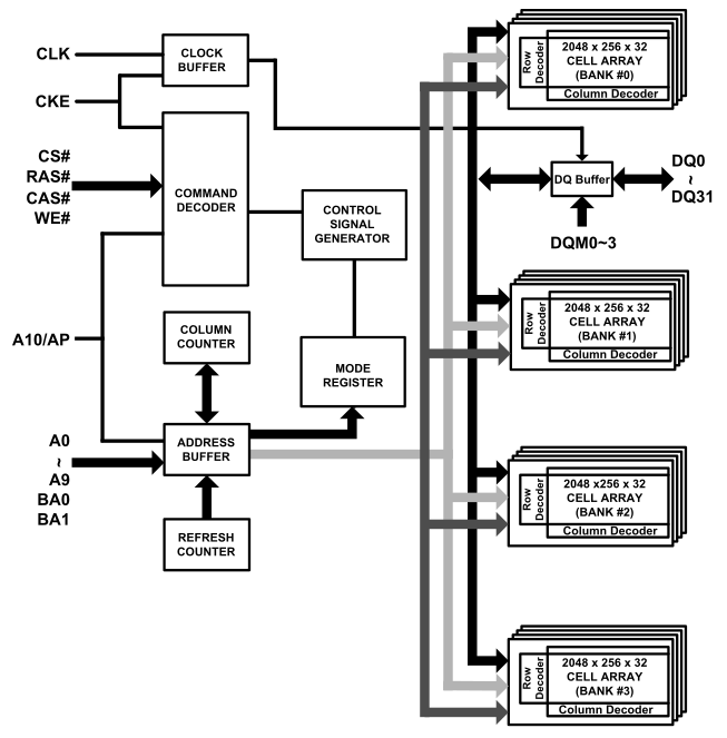
Figure 3 from EtronTech EM638325 datasheet
Architecture
DRAM initialization
Handling timing
The SDRAM is configured to operate in bursts of 8 to maximize throughput. This is great for interacting with cachelines that are configured to be 32 bytes (one burst) long, but complicates single word or sub word (1 or 2 bytes) accesses.
[TODO]
Simulation
To drive simulation of the SDRAM I used cocotb like I do for almost all of my digital design projects.
I created a black box python model of the SDRAM to act as the virtual memory store. This allows reading and writing data in the simulation to act like it will on the FPGA. This will be crucial when I am debugging the core later.
Architecture
Since the DOOMSoC memory bus will be implemented using AXI4, the port memory controller has an AXI4 slave port that it uses to receive memop from the system. The AXI4 burst is necessary to extraxt the maximum bandwidth (BL8) from the SDRAM.
The memory controller is implemented as a simpel state machine. unop reset it performs the mandatory initialization sequence for the SDRAM, and then begins servicing requests from the bus.
the MC translates memops into necessary DRAM control signals. The FSM implements a timer and will wait the specified number of cycles between the issue of particular DRAM commands.
...
[TODO: FSM diagrams]
AXI Port
doesnt quite respect the axi spec. both awvalid and arvalid are asserted at the same time only one op, read or write, will every be serviced in any particular cycle implicit guarantee from the AXI Masters to never issue reads and writes to the sdram simultaneously bus arbiter will guarantee that only one operation is sent to the memory controller is any cycle arbiter also performs interconnect-level serialization (no out of order support) interconnect should handle commands from master from BL1 to BL8 and convert them depending on the slave's capability