DOOMSoC Display Driver
Back to project overview
Intro
The HDMI connector on the Gowin Tang Nano 20K implements the DVI-D subset of HDMI. I.e. only four signals. One clock signal and three colors channels: red, green, and blue. For each pixel, the brightness value of each color channel is streamed to the display serially. Like most high-speed serial signals, it is not sufficient to simply stream the bits down the wire. Instead, each signal is electrically implemented as a differential pair and each 8-bit pixel value is converted to a stream of encoded symbols. The encoding scheme, called TMDS (Transition Minimized Differential Signaling), is used to minimize the number of transitions (to reduce RF bandwidth) and maintain DC balance.
Pixel Clock and Signal Timing
One pixel of the frame is sent to the display during each cycle of the pixel clock. The pixel clock's frequency must be chosen to display every pixel in the frame within a single frame time, typically 1/60Hz. However, the display driver does not just send visible pixels, it also sends blank signals at the borders of the image. As far as I know, this is entirely a legacy requirement, but a requirement nonetheless.
The formula for calculating pixel clock frequency is as follows:
Horizontal counts = h_active + h_front_porch + h_sync_pulse + h_back_porch
Vertical counts = v_active + v_front_porch + v_sync_pulse + v_back_porch
Pixel clock = Horizontal counts * Vertical counts * Refresh Rate
The blanking durations for 640x480@60Hz work out to be:
H_Total: 640 + 16 + 96 + 48 = 800 pixels
V_Total: 480 + 10 + 2 + 33 = 525 lines
p_clk: 800 * 525 * 60 = 25,200,000 Hz = 25.2 MHz
To stream pixels from the frame buffer, two counters, X and Y, are used to keep track of the current "beam" position.
As the X and Y counters tick up, they define different regions of the frame:
-
Active Video: This is the visible part of the screen. When the counters are in this zone, a Data Enable (DE) flag is raised. The current X/Y pixel is read from the frame buffer and sent to the TMDS encoders.
-
Blanking: When the "beam" reaches the edge of the screen, it needs time to return to the left side or the top. This is the blanking period, made up of the Front Porch, Sync Pulse, and Back Porch. During this time, DE is low, no pixel data is sent and the HSYNC or VSYNC signals are pulsed to tell the monitor to start a new line or frame.
Frame Buffer
Typically, a frame buffer is usually implemented as two separate buffers (double buffering). The display driver reads pixels from the front buffer while the graphics engine renders a new frame in the back buffer. Ideally, the new frame is completed sometime before the display driver is in the vertical blanking section. At this point, the front and back buffer are swapped, and the pixel values from the new frame begin streaming out to the display.
Since I am so limited by on-chip SRAM, I am unable to implement double buffering. In fact, I cannot fit even a single full resolution (640x480) truecolor frame. That would consume nearly 1 MB of memory, but I must work with ~100KB of BRAM.
Fortunately, DOOM used a basic video mode called VGA Mode 13h. This graphics mode used 8 bit pixel values to index into a 256-color palette.
As a result, a full DOOM frame consumes 320x200x8 = 64KB. I can fit this comfortably on chip. I may just have to suffer through some screen tearing. The alternative is to store the framebuffer in SDRAM. However I'd really like to avoid this as it might limit performance of the game engine. Plus the memory controller hasn't been written yet.
To imitate the VGA palette, I will create a small 256 x 18 bit BRAM connected to the system bus that holds the color palette that will be used to render pixels as the display engine is reading from the frame buffer.
Potential Optimization:
It seems like DOOM only used 14 different color palettes. A simple performance optimization might be to preload all palettes from the WAD at boot and quickly switch between them with a single instruction from the game engine.
Upscaling from VGA Mode 13h
Since the game is rendered at 320x200 but the display expects 640x480, some upscaling must be performed. To simplify things, I will not be doing any tradition upscaling, I will just be manipulating the frame buffer index calculations.
Using this method, scaling in the horizontal axis is easy as 640 is an even multiple of 320. simply double every pixel in the x-axis or alternatively drop the lowest bit from the x_position counter.
Scaling in the vertical axis is more complicated, as the scaling factor is 2.4. This can be approximated by multiplying by 1705 and then right shifting 12.
logic [8:0] x_scaled;
logic [7:0] y_scaled;

assign x_scaled = x_count[9:1]; // x * 2
assign y_scaled = (y_count * 1705) >> 12; // y * 2.4
TMDS Encoding
The 8-bit color values retrieved from the palette cannot be sent directly to the HDMI pins. To ensure reliable transmission, they must first be encoded into TMDS. This stage performs two critical transformations: it minimizes the number of bit transitions to reduce electromagnetic interference (EMI), and it maintains a "DC balance" to prevent the average voltage on the wire from drifting over time.
Each 8-bit color channel (red, green, and blue) is mapped to a 10-bit symbol. The encoding process works in two stages:
- Transition Minimization: The encoder applies either an XOR or XNOR operation across the bits of the input byte. By choosing the operation that results in the fewest bit transitions, the encoder reduces the high-frequency noise generated by the cable.
- DC Balancing: The encoder keeps a running tally of the difference between the number of 1s and 0s sent so far. If the stream becomes biased one way or the other, the encoder will invert the next symbol to pull the average voltage back toward zero.
During the blanking intervals, the encoders ignore the pixel data and instead encode the HSYNC and VSYNC control signals. These are mapped to four specific 10-bit control symbols that the monitor uses to identify the end of a line or frame. The blue channel typically carries the HSYNC and VSYNC signals, while the green and red channels just send encoded CTRL0.
Clock Generation and Serialization
Since one pixel is processed per clock cycle, but the pixel data must be transmitted serially over the HDMI cable. This serialization is implemented in hard IP on the Tang Nano. Each color channel gets its own serializer to take a 10-bit encoded symbol and "shift" it out one bit at a time.
Because HDMI typically uses Double Data Rate (DDR) I/O, the serializer outputs one bit on every edge of the s_clk. To move 10 bits of data per pixel, the serial clock must run at exactly 5x the frequency of the pixel clock. Since the pixel clock for 640x480@60Hz was previously calculated to be 25.2 MHz, the serial clock must be 126 MHz. To make sure the s_clk and p_clk remain in phase, I generate the 126MHz s_clk with an rPLL primitive and then divide it by 5 to generate the p_clk.
The proper PLL parameters can by found by running the gowin_pll tool.
Ex: gowin_pll -i 27 -o 126 -d 'GW2A-18 C8/I7':
rPLL #(
    .FCLKIN("27.0"),
    .IDIV_SEL(2),   // -> PFD = 9.0 MHz (range: 3-500 MHz)
    .FBDIV_SEL(13), // -> CLKOUT = 126.0 MHz (range: 3.90625-625 MHz)
    .ODIV_SEL(4)    // -> VCO = 504.0 MHz (range: 500-1250 MHz)
) sclk_pll_i (
    .CLKOUTP(),
    .CLKOUTD(),
    .CLKOUTD3(),
    .RESET(1'b0),
    .RESET_P(1'b0),
    .CLKFB(1'b0),
    .FBDSEL(6'b0),
    .IDSEL(6'b0),
    .ODSEL(6'b0),
    .PSDA(4'b0),
    .DUTYDA(4'b0),
    .FDLY(4'b0),
    .CLKIN(clk), // 27.0 MHz
    .CLKOUT(s_clk), // 126.0 MHz
    .LOCK()
);
CLKDIV #(
    .DIV_MODE("5")
) clkdiv_inst (
    .HCLKIN(s_clk),
    .RESETN(~reset),
    .CALIB(1'b0),
    .CLKOUT(p_clk)
);
The Serializers are implemented as follows:
OSER10 oser_inst (
    .Q(serial_out),
    .D0(symbol_data[0]),
    .D1(symbol_data[1]),
    .D2(symbol_data[2]),
    .D3(symbol_data[3]),
    .D4(symbol_data[4]),
    .D5(symbol_data[5]),
    .D6(symbol_data[6]),
    .D7(symbol_data[7]),
    .D8(symbol_data[8]),
    .D9(symbol_data[9]),
    .PCLK(p_clk),
    .FCLK(s_clk),
    .RESET(reset)
);
Implementation:
Here is a complete block diagram of the display driver module.
graph TD

    SC[System Clock]
    PLL[PLL]
    CDIV[Clock Div]

    IN["Memory Bus (AXI)"]
    TGEN[Timing Generator]
    SCALE[Index Scaling]
    FB[Frame Buffer]
    PL[Palette]

    subgraph TMDS_Encoding
        ENC_B[Blue Encoder]
        ENC_G[Green Encoder]
        ENC_R[Red Encoder]
    end

    subgraph Serializers
        SER_P[Pclk Serializer]
        SER_B[Blue Serializer]
        SER_G[Green Serializer]
        SER_R[Red Serializer]
    end

    IN --->|New Frame Data| FB
    IN --->|Palette Data| PL
    TGEN --->|Pixel Count| SCALE
    SCALE --->|Scaled Pixel Count| FB
    FB --->|Palette Index| PL
    PL --->|Blue Value| ENC_B
    PL --->|Green Value| ENC_G
    PL --->|Red Value| ENC_R

    ENC_B -->|Blue Symbol| SER_B
    ENC_G -->|Green Symbol| SER_G
    ENC_R -->|Red Symbol| SER_R

    SC -.->|clk| PLL
    PLL -.->|s_clk| Serializers
    PLL -.->|s_clk| CDIV
    CDIV -.->|p_clk| TGEN
    CDIV -.->|p_clk| TMDS_Encoding
    CDIV -.->|p_clk| FB
    CDIV -.->|p_clk| PL
    CDIV -.->|p_clk| SER_P

    SER_P ---> pclk
    SER_B ---> blue
    SER_G ---> green
    SER_R ---> red
Testing
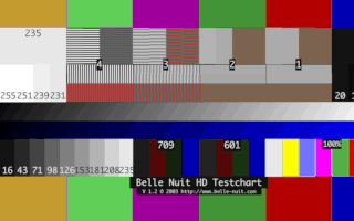
For my initial test, I converted a test image I found on Google to use the default DOOM color palette. I had Gemini write a Python script to take the original PNG and quantize it based on the values available in the color palette. I then rendered it back out using the palette to produce this png:
I loaded both the image and palette data into ROMs on the FPGA and connected them to the display driver. This is the result shown on my display:
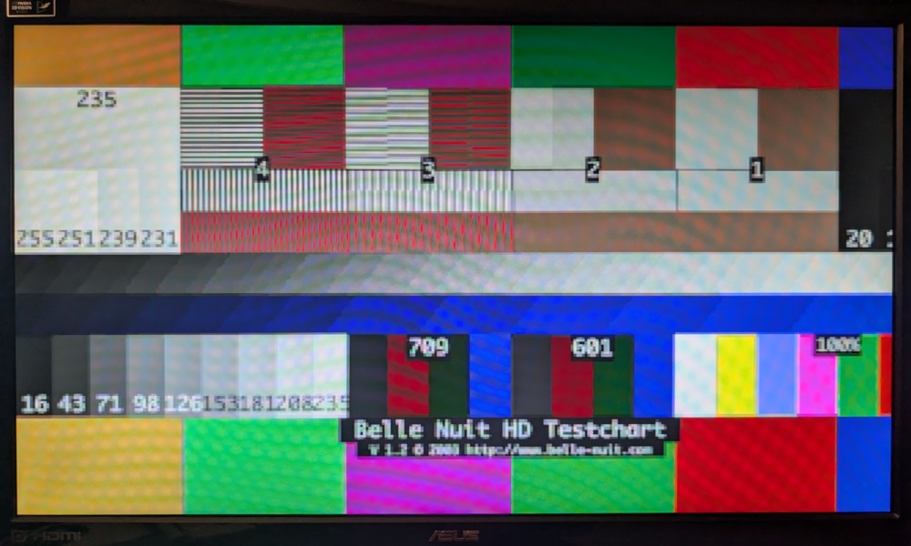
I consider the basic display driver a success.